Within the ever-evolving realm of high-speed networking, the progression of 800G OSFP optical transceivers emerges as a testament to innovation and advancement. From its inception to its current state, the evolution of 800G OSFP modules demonstrates the steadfast pursuit of swifter data transmission, expanded bandwidth, and improved performance within contemporary data centre environments. This article mainly shows the evolution route of 800G OSFP optical transceivers.
800G OSFP Optical Transceiver Evolution Route
Route 1: EML Route
The 800G DR8 OSFP optical transceiver integrates eight 100G EML lasers, representing a mature solution with robust performance. However, due to the high number of lasers, it incurs relatively higher costs. Looking ahead, advancements are anticipated to enable the realization of 800G DR4 OSFP, halving the laser count and consequently reducing costs. Long-term projections foresee the possibility of pricing approaching that of 400G optical modules.
The 800G DR8 OSFP optical transceiver, which integrates eight 100G EML lasers, represents a mature solution with robust performance. However, it incurs relatively higher costs due to the high number of lasers. Looking ahead, advances are anticipated to enable the implementation of 800G DR4 OSFP, halving the laser count and consequently reducing the cost. Long-term projections foresee the possibility of pricing close to that of 400G optical modules.
Route 2: Silicon Photonics Route
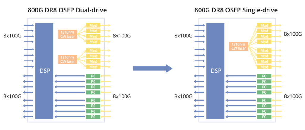
At present, 800G silicon photonics utilizes a dual-laser drive method, leveraging the existing 400G DR4 solution for cost efficiency compared to EML alternatives. Looking forward, advancements will drive a transition to a single-laser driving approach, integrating a thin-film lithium niobate modulator to minimize optical path loss. The single-laser solution in silicon photonics is set for mass production by 2025, offering further cost reductions for the 800G DR8 silicon optical module. Nonetheless, the dual-laser approach continues to dominate the mainstream for silicon photonics.

800G 2xFR4 OSFP Evolution Route
The current 800G 2xFR4 OSFP configuration utilises two sets of 4-wavelength CWDM 100G EML lasers, each consisting of 4 lasers. However, future advancements will transition towards an FR4 setup employing 4 CWDM wavelength 200G EML lasers.
This shift to 800G FR4 necessitates using 4-wavelength CWDM lasers in silicon photonics solutions, eliminating any cost advantage. Currently, the dominant preference lies with EML schemes, with no ongoing exploration of silicon photonics schemes by manufacturers. The FS 800G 2xFR4 OSFP transceiver features cutting-edge features such as a self-developed 53G EML laser chip and a built-in Broadcom 7nm DSP chip, ensuring unparalleled performance and reliability.
800G SR8 OSFP Evolution Route
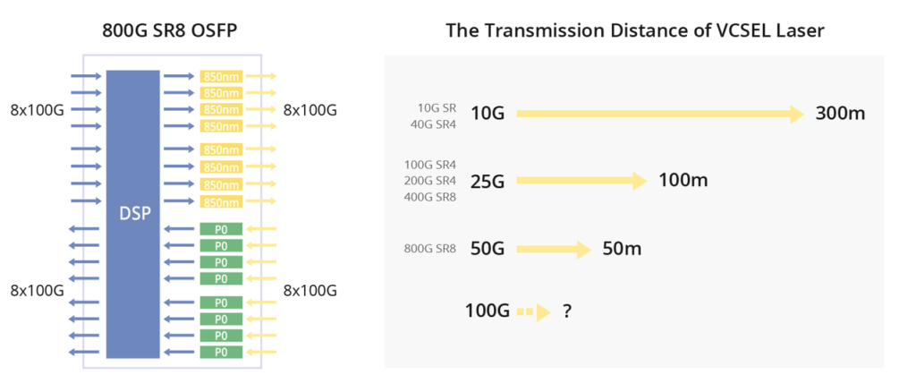
Eight VCSEL lasers with a 50-meter transmission range are used in the 800G OSFP SR8 module. Due to the small distance, the application scenario is more constrained than the 400G SR8. We can observe that the shorter the transmission distance of a VCSEL laser, the larger its single-channel rate, by comparing the transmission distances of 10G, 25G, 50G, and 100G SR optical transceiver modules.
As the single-channel rate of optical modules increases, the VCSEL technology is reaching a bottleneck. Anticipating the era of 1.6T optical modules, VCSEL lasers may further limit the transmission distance. For cost-effective solutions, customers may find 1.6T cable options more favourable. As a result, the presence of VCSEL lasers in the 1.6T optical module market is expected to diminish in the future. The FS 800GBASE-SR8 OSFP optical transceiver is compliant with IEEE P802.3ck, OSFP MSA standard. Built-in digital diagnostic monitoring (DDM) allows access to real-time operating parameters. It is also suitable for 800G Ethernet, data centre and Breakout 2x 400G SR4 applications.

From CPO to LPO
CPO Solution
The CPO solution stands out in that it eliminates one DSP chip, thereby reducing power consumption and cost. It innovatively integrates the switching chip, which is responsible for the optoelectronic conversion, directly onto the optical module via co-encapsulation. This integration minimises electrical signal loss, reducing latency and overall power consumption. However, challenges arise regarding the co-packaging logistics and repair protocols for malfunctioning optoelectronic chip clusters, potentially delaying large-scale production and application for up to three years or remaining indefinitely in the conceptual phase.
LPO Solution
The LPO solution reduces power consumption by utilizing LPO linear direct drive technology and high linearity TIA and DRIVER chips. However, it compromises system error rate and transmission distance, rendering it suitable for specific applications. It depends on enhancements to switching chip performance and may potentially achieve transmission distances of up to 500m in the future, evolving into a viable solution for data centres.
Essentially, the LPO represents the evolutionary path of pluggable optical modules in terms of packaging. It provides a more straightforward and reliable alternative to the CPO solution.
Continuing the Exploration of 800G OSFP
Embarking on a journey through the evolution of 800G OSFP optical transceivers unveils a landscape shaped by innovation and technological prowess. As we navigate our way toward faster data transfer, expanded bandwidth, and improved performance, the diverse pathways showcased here underscore the dynamic nature of modern data centre environments. With each advancement, we edge closer to unlocking new possibilities and reshaping the future of high-speed networking. Continue to explore FS and embrace the transformative power of innovation.
Related Articles:
Unlocking Next-Gen Connectivity with the 800G OSFP Transceiver
AI Computing Accelerates the Deployment of 800G Optical Transceiver


